Microstructures
by
George
Langford, Sc.D., Massachusetts Institute of Technology, Cambridge, MA,
1966
Copyright©2005 by George Langford
Non Ferrous Alloys - Lesson 3 -
Eighth specimen

|
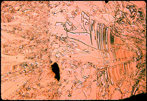
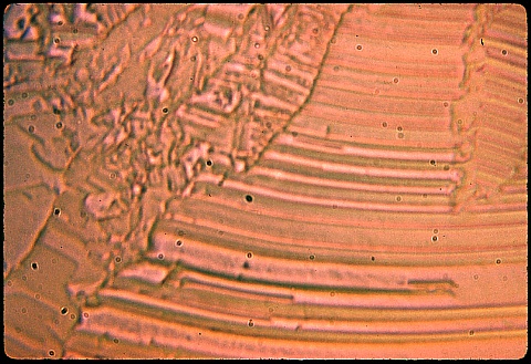
This photomicrograph was taken at 200X, and the next one is
at 1000X. The etchant was ammonium peroxide - hydrogen
peroxide. The material is copper.
How was this microwave guide formed ?
Why would you say it was not cast ?
The wave guide was made on a pattern made
from
poly(methyl methacrylate) - PMMA - and coated with silver. It was
then
electroplated heavily with copper from a copper sulphate bath.
This
particular specimen was removed from the bath several times, producing
a layered structure.
|

|
The bent "annealing" twins are indicative of a highly
faulted and strained microstructure, a result of the high deposition
rate necessary to form such a massive electrodeposited thickness (six
millimeters). Note the absence of any normal grain structure, the
columnar grains, and the lack of porosity.
This excellent microstructure was produced by a process called electroforming (no
endorsement intended). The silver was leached away by acid
treatment from the inside of the waveguide after removing the PMMA with
a solvent.
Specimen 9 is next on the agenda.
|

